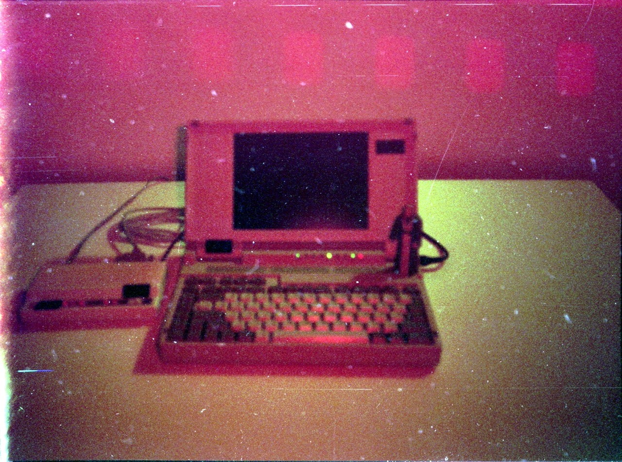
It’s a good candidate since it sounds like there’s no precision mechanical components like there would be in a hard drive. Does anyone have ideas for how I’d go about this? Is there a barrier I’m not considering?
I know how to make basic semiconductors already, so that’s not an issue.
Edit: I’ve got an answer written down in the comments now. TL;DR you’d still need lithography to do it the OG way, because of the patterned magnetic material that directed bubbles around the medium, but material requirements are actually pretty flexible.
A lot of things that we assume can only be made by giant complexes of high-tech equipment were first prototyped by hand on a workbench. This sounds like a great project.
(I don't know anything about the details of bubble memory. It's entirely possible this is impossible. Certainly worth looking into though.)
Just from a quick Google search, it looks like it's similar to tape memory, except the data moves along the tape, instead of the tape moving over the reading head. According to
 diagram by TI, it looks like the bubbles are on some iron wafer and forcibly moved around by two coils. Then, on a second substrate there are some type of read & write head.
So here's how I would go about this: first, I'd wrap some small metal plates in insulated magnet wire, place two permanent magnets on the top and bottom (sandwich style) and stick a read head on the edge of the plate. Then you push AC current through the two coils offset by 90 degrees. This should push the bubble in a circle, and that can be read by the tape head.
Keep in mind though, this is a complete guess based on a simplified diagram from the 70s. I don't actually know if this is how they work.
Do you understand the physics of the bubble itself at all? I'm a bit unclear on how a this pushes around domain walls in the first place. Like, it makes a kind of sense, electrons hold spin and they're moving, but the actual physical rate at which they do that is pretty low for even large currents. I take it it's a magnetic field itself that moves them based on what you wrote? How does that not erase anything?
It does look like two big coils in the diagrams. I wonder if the edge of the wafer was kept "empty" for bubbles to move in and out of, then.
I know how to make basic semiconductors already, so that's not an issue.
Uh, do you mean you know how to design them and send them somewhere to be made, or do you actually make them yourself? I thought you needed a crazy manufacturing plant for that.
As for making bubble memory, have you considered the material requirements? It looks like bubble memory used gadolinium gallium garnet, or yttrium iron garnet. Additionally, it sounds like bubble memory is significantly more complex than you'd think because while there aren't any mechanical components, it sounds like there are moving components.
Sam Zeloof has made chips in his garage and posted a whole series about it on Youtube. He bought his silicon wafers, he didn't grow them, and his machines do take up the whole garage - but he did the whole thing himself. Fascinating viewing IMO. I don't know anything about where one would get these garnetty materials you mention, though.
So, I'm still doing research, but it seems like any ferrimagnetic thin film should work.
Rare earths would have been in lower demand at the time I think, some garnets have useful magnetic properties, and growing garnets is relatively easy. Similar synthetic crystals are common as lasing mediums now.
Uh, do you mean you know how to design them and send them somewhere to be made, or do you actually make them yourself? I thought you needed a crazy manufacturing plant for that.
Here's a link to my favourite YouTuber, Sam Zeloof, on Invidious! If you want to see him actually do it, the "Transistor Step By Step" video is good.
As for making bubble memory, have you considered the material requirements? It looks like bubble memory used gadolinium gallium garnet, or yttrium iron garnet.
That's one of the big questions. Do I need exotic materials, or were they just better from the perspective of a 1970's manufacturer? If I can make a bad one with some kind of ferrite that's still something.
Additionally, it sounds like bubble memory is significantly more complex than you’d think because while there aren’t any mechanical components, it sounds like there are moving components.
If it's a matter of electrical control, though, that becomes an analytical problem which I'm pretty good at. I also have the advantage of access to 2020s electronics, so if I need to measure or control things on the order of microseconds it's no big deal.
Basic semiconductors… like ICs?
Really bad ones with visible-sized features, yes. I linked a YouTube channel elsewhere in here.
When someone says basic semiconductor, my first thought would be a single diode or maybe a transistor, not an entire integrated circuit.
Maybe there's a YouTube tutorial
There… actually is some promising looking videos. I did not expect that, this is a pretty damn forgotten technology.
Thanks!


