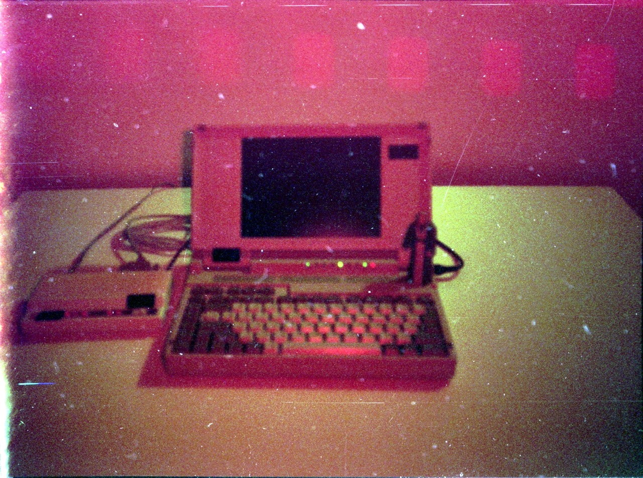
It’s a good candidate since it sounds like there’s no precision mechanical components like there would be in a hard drive. Does anyone have ideas for how I’d go about this? Is there a barrier I’m not considering?
I know how to make basic semiconductors already, so that’s not an issue.
Edit: I’ve got an answer written down in the comments now. TL;DR you’d still need lithography to do it the OG way, because of the patterned magnetic material that directed bubbles around the medium, but material requirements are actually pretty flexible.


Do you understand the physics of the bubble itself at all? I'm a bit unclear on how a this pushes around domain walls in the first place. Like, it makes a kind of sense, electrons hold spin and they're moving, but the actual physical rate at which they do that is pretty low for even large currents. I take it it's a magnetic field itself that moves them based on what you wrote? How does that not erase anything?
It does look like two big coils in the diagrams. I wonder if the edge of the wafer was kept "empty" for bubbles to move in and out of, then.